KOR v1: a 9 V active buffer and boost for an HHH Strat, as SMD and THT boards
A small op-amp preamp that sits between the Volume pot and the jack without touching the guitar's wiring: it isolates the cable from the humbuckers, adds up to 7.7 dB of boost on a trimmer, and a 3PDT switch turns it into true bypass with zero current. A 32×20 mm SMD and a 48×28 mm THT version, ngspice simulations and a wiring diagram.
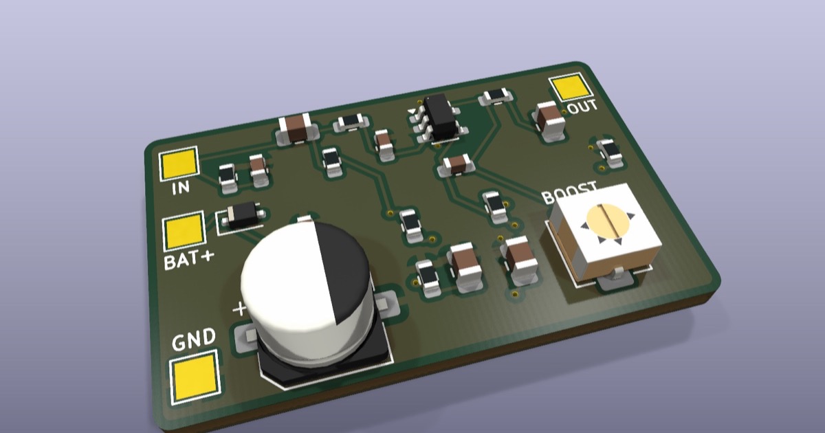
I designed a small active preamp for my three-humbucker (HHH) Strat: KOR v1. It leaves the guitar's wiring alone. The 5-way selector, Volume and Tone stay as they are, and no new pot is added. The board goes between the Volume output and the jack and does two things: it isolates the cable from the pickups (buffer), and it can raise the signal by up to 7.7 dB (BOOST). One mini switch added to the pickguard switches the guitar between active and passive. In passive mode the preamp is completely out of the signal path and the battery draws no current at all.
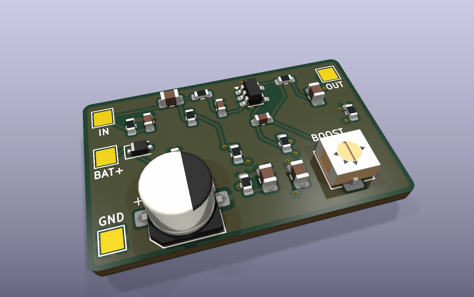
There are two versions of the board: a 32×20 mm SMD board and a 48×28 mm THT board for hand soldering. The circuit is the same; only the op-amp and the packages differ.
Why a buffer?
In a passive guitar the pickup, the pots and the cable form a filter together. The humbucker's inductance of about 4.5 H resonates with the cable capacitance (about 300 pF for a 3 m cable), and the treble above that resonance falls off quickly. The longer the cable, the lower the resonance and the darker the sound.
The buffer hides that capacitance from the pickup. The pickup now sees only the board's input and a few centimetres of wire; the op-amp drives the cable. I compared the two cases in ngspice with a humbucker model (4.5 H, 9 kΩ, 200 pF), 500k Volume and Tone pots, a 22 nF tone capacitor, a 3 m cable and a 1 MΩ amp input:
| Passive | Active (BOOST 0 dB) | |
|---|---|---|
| Resonant peak | 3.1 kHz, +5.1 dB | 3.7 kHz, +3.7 dB |
| 5 kHz | -3.4 dB | +0.6 dB |
| 10 kHz | -18.1 dB | -14.2 dB |
So the peak moves up by about 600 Hz and about 4 dB more treble survives around 5 kHz. The difference grows when the Volume is turned down: in a passive guitar the turned-down pot and the cable form a low-pass filter and the sound gets muffled. In active mode the op-amp drives the cable, so that effect goes away.
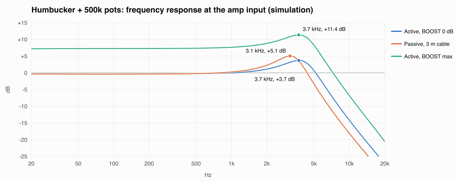
Not everyone wants that extra brightness. The darkness of the passive sound comes from the cable, so I left an empty spot on the board for it: C9, a capacitor from the input to ground. Fitting a 220-470 pF NP0 there puts the cable capacitance back and brings the sound closer to passive. It is not fitted by default.
The circuit
9V ── D1 (reverse polarity) ── 47µ ‖ 100n ── VCC
VCC ── 100k ── VREF (≈4.4 V, 10µ) ── 100k ── GND

IN ── 10M ── GND
IN ── 47n ──┬── 1M ── VREF
            └── 1k ── (100p → GND) ── op-amp +
op-amp − ── 33k ── 10µ ── GND
op-amp out ── RV1 47k (BOOST) ── op-amp −   (100p in parallel)
op-amp out ── 100 Ω ── 10µ ──┬── OUT
└── 100k ── GND- Single supply and virtual ground: two 100k resistors take half of the 9 V battery, filtered by 10 µF. The op-amp input is tied to this voltage through 1 MΩ.
- Input: the 47 nF input capacitor blocks DC. The 10 MΩ holds the input at ground. Both ends of the capacitor always sit at a defined voltage, which reduces the pop when the switch is flipped. 1 kΩ + 100 pF filter out radio frequencies before they reach the op-amp. The input impedance is a little under 1 MΩ, so it does not load the pickup more than a passive amp input does.
- Gain: a non-inverting amplifier with a gain of 1 + RV1 / 33k. With the trimmer fully left it is 0 dB (a pure buffer); fully right it is 1 + 47/33 = 2.42, or +7.7 dB. The 10 µF in the feedback leg applies the gain to AC only, so the output's DC level stays at VREF. The parallel 100 pF lowers the gain in the ultrasonic range and keeps the op-amp stable.
- Output: 100 Ω isolates the op-amp from the cable capacitance. 10 µF blocks DC, and 100k discharges the output capacitor.
- Reverse polarity: if the battery is connected backwards, a Schottky diode (BAT54J on the SMD board, BAT85 on the THT board) blocks the current. The diode drops about 0.1 V, so the op-amp runs at 8.9 V.
How much signal does it take?
The op-amps are rail-to-rail. In simulation the output swings cleanly up to ±4.35 V on the 8.9 V supply. With BOOST at maximum the input does not clip up to 1.8 V peak; at 2 V the output hits the rail. With BOOST at 0 dB the limit rises to 4.4 V peak. The board is meant as a clean buffer and boost, not a distortion.
Two versions: SMD and THT
| SMD | THT | |
|---|---|---|
| Board | 32×20 mm, 2 layers | 48×28 mm, 2 layers |
| Op-amp | OPA170AIDBVR (SOT-23-5) | TLV2371IP (DIP-8, socketed) |
| Current | ~155 µA | ~0.6 mA |
| Always on, 9 V battery | ~3000 hours | ~800 hours |
| BOOST trimmer | Bourns 3314J | Bourns 3296W (multi-turn) |
| Diode | BAT54J | BAT85 |
The current figures come from behavioural models of the op-amps (open-loop gain, gain-bandwidth and quiescent current) plus the rest of the circuit. Battery life assumes an alkaline 9 V battery of about 500 mAh.
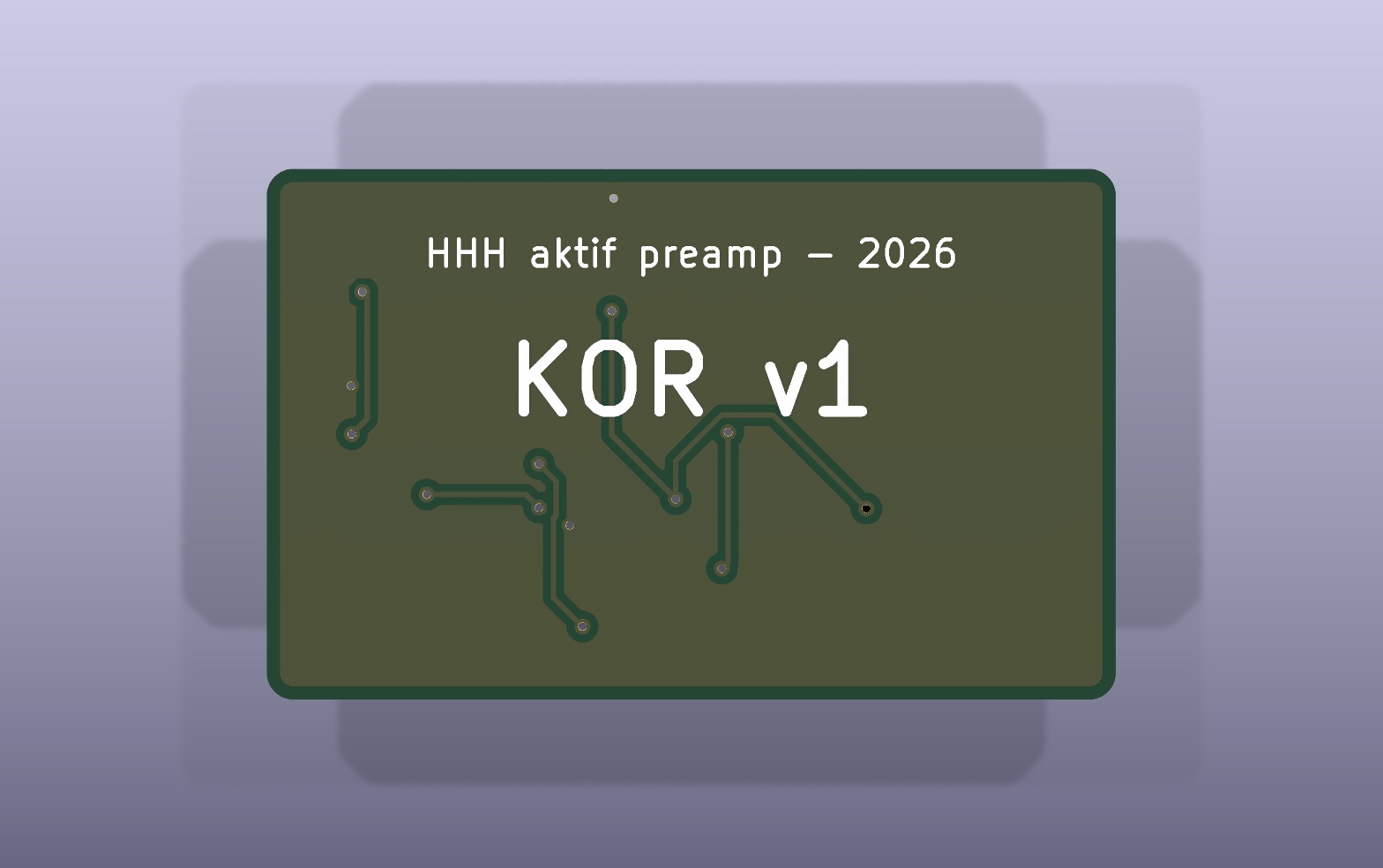
The back of the SMD board is all GND. The board is stuck into the cavity with double-sided foam tape. Even though the back is ground, the bottom should be insulated with heat-shrink or Kapton tape so that a wire or screw in the cavity cannot touch it.
On the THT version the resistors lie flat and the op-amp sits in a DIP-8 socket. The electrolytics (C1, C5, C7, C8) are polarised: the long leg goes into the square pad marked "+" on the silkscreen. 5 mm electrolytics are usually 11 mm tall; if the cavity is not deep enough, solder them lying down. The assembly order I suggest: resistors and diode, disc capacitors, socket, film capacitor, trimmer, electrolytics, and the op-amp last.
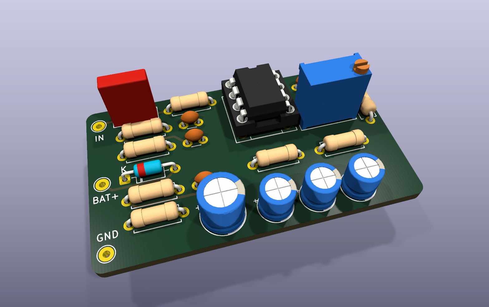
Both boards have the same pads: IN, OUT, GND, BAT+, so the wiring does not change. KiCad DRC reports 0 errors and 0 unconnected pads on both.
Wiring
A mini 3PDT on-on switch (9 lugs) is added to the pickguard. Each of the three poles has its own job:
              3PDT switch (each pole: top / MIDDLE=common / bottom)
              ON = top, OFF = bottom

Pole A (output):   top ── PCB OUT
                   MIDDLE ── Jack TIP
                   bottom ── Volume wiper

Pole B (input):    top ── Volume wiper
                   MIDDLE ── PCB IN
                   bottom ── unused

Pole C (battery):  top ── PCB BAT+
                   MIDDLE ── battery (+)
                   bottom ── unused

Battery (−) ── PCB GND ── guitar common ground (pot bodies, Jack SLEEVE)- OFF: the Volume output goes straight to the jack. The preamp input is disconnected and the battery is cut off completely: true bypass and zero current.
- ON: the signal goes through the board.
- The mono jack found in most Strats can stay. In that case the battery is cut by the switch, not the jack, so the switch should be set to OFF when the guitar is not in use. If you prefer, make the jack stereo (TRS) and connect the battery minus to the ring; then pulling the cable also cuts the battery.
- The lug layout of mini 3PDT switches varies by brand. Before wiring, check with a multimeter which lug connects to the common lug in which position.
- Shield the cavity and the underside of the pickguard with copper foil and connect the foil to GND. An active circuit is more sensitive to noise than passive wiring.
To verify on the prototype
The boards have not been made yet. All the numbers above come from simulation and calculation. When the boards arrive I will check:
- The tone difference between ON and OFF on a real guitar, and the right value for C9.
- Pop when the switch is flipped.
- Hum and noise with and without shielding.
- Current: whether the estimates of 155 µA with the OPA170 and 0.6 mA with the TLV2371 hold on a real board.
- Whether hard picking clips with BOOST at maximum.
Download
| File | Contents | Size |
|---|---|---|
| kor-v1-smd-kicad.zip | KiCad 10 project (SMD): schematic, PCB, DRC report, schematic PDF, Gerber, BOM and CPL (pos_ust.csv), 3D renders, wiring note | 0.9 MB |
| kor-v1-tht-kicad.zip | KiCad 10 project (THT): schematic, PCB, DRC report, schematic PDF, Gerber, BOM, assembly PDF, 3D renders, wiring note | 0.9 MB |
| kor-v1-smd-gerber.zip | Gerber + Excellon only for the SMD board, ready to upload to JLCPCB | 31 KB |
| kor-v1-tht-gerber.zip | Gerber + Excellon only for the THT board, ready to upload to JLCPCB | 17 KB |
The projects use only footprints from KiCad's standard libraries, so there is nothing extra to install. For JLCPCB assembly of the SMD board, the BOM and CPL files are in the production/ folder. Check part orientation in the assembly preview: KiCad and JLCPCB define 0° differently for some packages. The wiring note inside the packages is in Turkish.
Comments
Be the first to comment.
Sign in with your Google account to comment. Your name and comment are public. Your email and IP address are kept to deal with abuse, but never shown.