BEY-HAN Overdrive: an 18 V MOSFET overdrive pedal inspired by the Marshall JVM
A tube-preamp character from four BS170s, a 17 V rail doubled from 9 V, trimpot-free bias, a Marshall tone stack and all through-hole parts: the circuit, the board and the road to Rev 2.2 of BEY-HAN Overdrive.
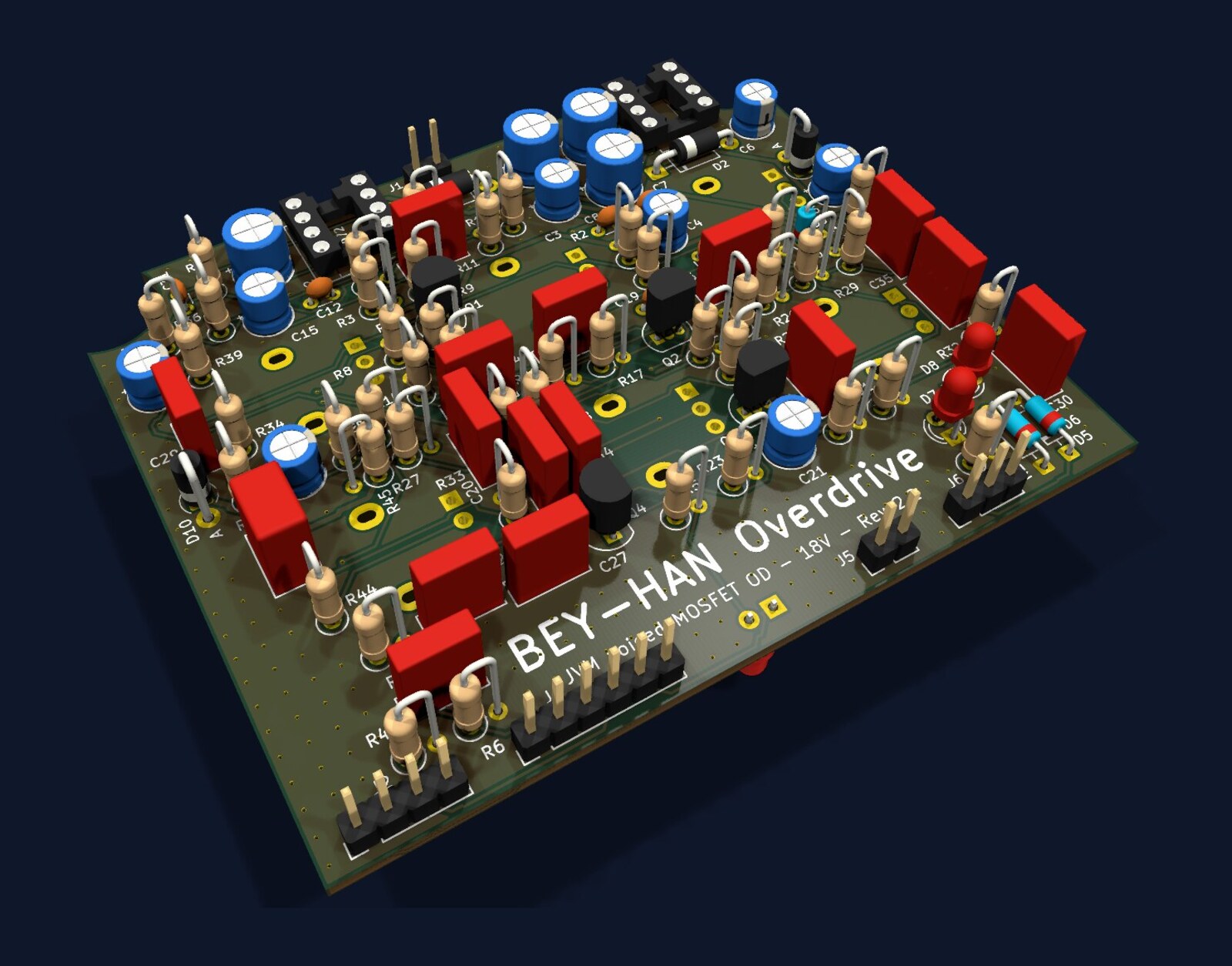
BEY-HAN Overdrive is a guitar pedal I designed after the OD channel of the Marshall JVM410H. It uses four BS170 MOSFETs to imitate the clipping character of a tube preamp, runs internally at about 17 V (doubled up from 9 V) for more headroom, and every part is through-hole, so anyone with a soldering iron can build it. The board is 84 × 70 mm, two layers, and fits a Hammond 1590BB enclosure.
In this post I go through the circuit stage by stage, then how the board was laid out, what changed from Rev 1 to Rev 2.2 and why, and how I verified the design. The project is drawn in KiCad 10; for this post I regenerated the 3D renders and re-ran the checks with kicad-cli straight from the board files.
Why MOSFETs, why 18 V?
Tube overdrive sounds different from transistor distortion: the clipping starts softly, the signal clips asymmetrically, and even harmonics (2nd, 4th) are prominent. The near square-law transfer curve of a JFET or MOSFET is much closer to that behaviour than a pair of diodes is. The BS170 is a cheap, ubiquitous N-channel MOSFET in a TO-92 package, and every gain stage in this pedal is built from it.
The 18 V is about headroom. A MOSFET stage running on 9 V compresses even the clean signal early: the tone gets muddy and the "clean but warm" region at low gain disappears. The pedal raises 9 V to about 17 V internally with a charge pump. In simulation, every stage keeps at least 5 V of swing even in the worst case.
The signal path
Input buffer
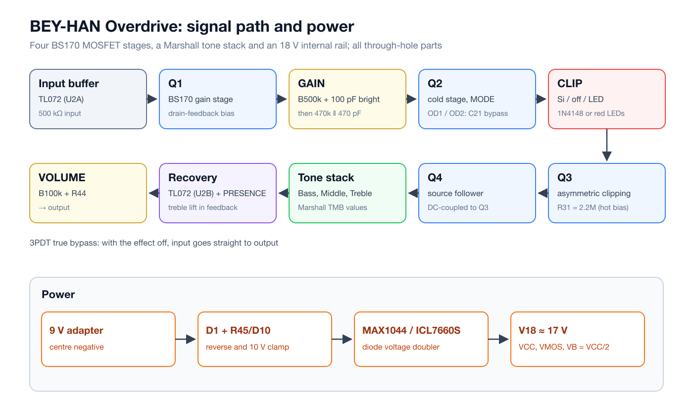
The guitar signal first reaches half of a TL072 (U2A). The op-amp runs as a voltage follower; its input is tied to half supply (VB = VCC/2) through 1M, and with the 1M pulldown in front of it the input impedance is 500 kΩ. That is high enough for passive pickups, and the follower gives a low output impedance to drive what comes next.
Q1: the first gain stage
The buffer output goes through 47 nF and 68k to Q1's gate. The 68k is a gate stopper that tames RF and oscillation. Q1 has a 10k drain resistor and 1k + 470 Ω in the source, with the 470 Ω part bypassed by 10 µF, so the AC gain is higher than the DC gain.
The key detail in this stage is the bias. The BS170's threshold voltage varies from part to part between 1 and 3 V. With a fixed gate voltage, every board would need a trimpot. Instead I used drain-feedback bias: the gate is fed from the drain through two 1M resistors whose midpoint is decoupled to ground with 100 nF. At DC the stage finds its own operating point (if the drain rises, the gate rises, the transistor conducts more, and the drain falls back); at AC the capacitor shorts out the feedback, so the gain doesn't drop. The pedal has no trimpots at all.
GAIN and bright
Q1's drain feeds the top of the GAIN pot (B500k) through 22 nF. A 100 pF capacitor sits between the top lug and the wiper: the classic bright cap that lets treble bypass the pot at low gain settings. After the pot the signal reaches Q2 through 470k ‖ 470 pF, the same coupling found in Marshall preamps, which trims the lows a little and brings the upper mids forward.
Q2: the cold stage and MODE
Q2 is deliberately run cold: a 33k drain resistor and 1k + 3.3k in the source. Drawing little current, this stage clips one side of the waveform early. The 4.7 µF capacitor that bypasses the 3.3k part of the source resistor is wired to the MODE switch:
- OD1 (switch open): no bypass, less gain. Clean up to about half the pot, then it opens up.
- OD2 (switch closed): bypass in, more gain; crunch even at low gain settings.
With the switch open, the 100k R42 keeps the capacitor charged, so flipping MODE doesn't pop. The 1 nF at Q2's drain is the first treble filter.
The CLIP selector
After Q2, the signal reaches the three-position CLIP switch through 10k:
| Position | What clips | Character |
|---|---|---|
| Si | two 1N4148s (anti-parallel) | tight, symmetric, the most compressed |
| OFF | no diodes, only the MOSFETs | the most open and dynamic |
| LED | two red 3 mm LEDs | higher clipping threshold, louder |
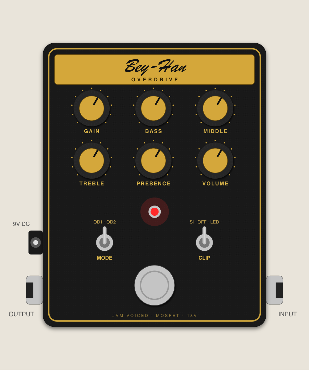
The Si position is symmetric on purpose; Q3 carries the asymmetry. The LEDs stay inside the box and are not visible on the lid.
Q3: asymmetric clipping
Q3 also uses drain-feedback bias, but its gate is additionally tied to ground through 2.2M. In Rev 2 that resistor was 1M. At 2.2M, Q3 runs a little hot and clips the two halves of the waveform at different points. In simulation, at full distortion the ratio of even to odd harmonics went from 0.24-0.33 to 0.7-1.6. One resistor value, and the harmonic balance moves much closer to a tube preamp.
Q4: source follower
Q3's drain is DC-coupled to Q4's gate (through 10k, no capacitor). This is the MOSFET counterpart of the cathode follower that sits before the tone stack in Marshall amps: Q4 gives no voltage gain, but it drives the passive tone stack from a low impedance, so the earlier stages' gain doesn't change however the tone stack loads it.
The Marshall tone stack
After Q4's source and a 1 µF coupling cap comes the classic Marshall TMB tone stack: 470 pF on treble, 22 nF on bass and middle, a 33k slope resistor; TREBLE B250k, BASS B250k, MIDDLE B25k. This network has its own personality: the three pots interact, and even with all of them at noon there is a noticeable dip in the mids. Part of the Marshall sound comes straight from here.
Recovery and PRESENCE
The tone stack loses a lot of level. To win it back, the second half of the TL072 (U2B) runs as a non-inverting amplifier with 4.7k / 22k feedback and 2.2 nF across the feedback resistor, so the amplifier itself rolls off the extreme highs slightly.
PRESENCE works much like the presence control on an amp: it adds a 2.2k + B50k pot + 47 nF path to the ground side of the feedback network. As the pot opens, feedback drops at high frequencies and gain rises; presence lifts the treble not by equalising but by loosening the feedback with frequency. In an amp that control sits in the power stage's feedback loop; here the same idea lives in the op-amp's loop.
VOLUME and true bypass
Finally: 10 µF, the VOLUME pot (B100k), a 100 Ω series resistor and a 100k pulldown on the output. The 3PDT footswitch does true bypass: with the effect off, the input jack connects straight to the output jack and the circuit never touches the signal. The footswitch's third pole lights the status LED.
Controls
| Left | Centre | Right | |
|---|---|---|---|
| Top row | GAIN (B500k) | BASS (B250k) | MIDDLE (B25k) |
| Bottom row | TREBLE (B250k) | PRESENCE (B50k) | VOLUME (B100k) |
All pots are B (linear) taper, because those are the easiest to find in 9 mm Alpha pots. GAIN and VOLUME need to behave logarithmically to feel natural, so I added taper resistors between the wiper and ground: R43 (47k) for GAIN and R44 (10k) for VOLUME. A resistor of roughly a tenth of the pot's value from wiper to ground bends a linear pot's curve towards a log one. If A500k or A100k pots are available, these resistors are simply left out.
Power: from 9 V to 17 V
The power chain needed as much care as the signal path:
- D1 (1N5817): a series Schottky diode. Plug the adapter in reversed and nothing happens; the pedal just doesn't work. Being a Schottky, it drops only ~0.3 V.
- R45 (22 Ω, 0.5 W) + D10 (BZX85C10): overvoltage protection. The charge pump chip tolerates at most 10.5 V, while unregulated "9 V" adapters can give 12-13 V unloaded. The 10 V zener clamps that. At 12 V the zener draws about 77 mA and 0.8 W, at 13 V 123 mA and 1.2 W; hence a 1.3 W zener and a 0.5 W series resistor. In normal use only ~0.3 V drops across R45.
- U1 (MAX1044 or ICL7660S): a charge pump normally used to make a negative voltage. I don't use its output here; instead, two Schottky diodes (D2, D3) turn it into a voltage doubler: while the bottom of the pump capacitor swings between 0 and 9 V, its top swings between 9 and 18 V, and D3 passes that peak onto the V18 rail. With BOOST connected, the pump runs at around 35-60 kHz, far above the audible band.
- V18 → VCC → VMOS: 10 Ω and 100 Ω resistors with 100 µF capacitors form RC filters that separate the op-amp and MOSFET supplies from each other and from the pump. VB is VCC halved by two 47k resistors.
- D9 (1N4148): across the pump's unloaded negative output, to ground. A precaution recommended in the Renesas and Maxim datasheets: it keeps that output from rising above ground and pushing the chip into latch-up.
In simulation, pump noise at the output is -102 dBV at 10 kHz in the worst case, and below -160 dBV at 45 kHz with BOOST. The whole pedal draws about 17 mA from the adapter.
The board
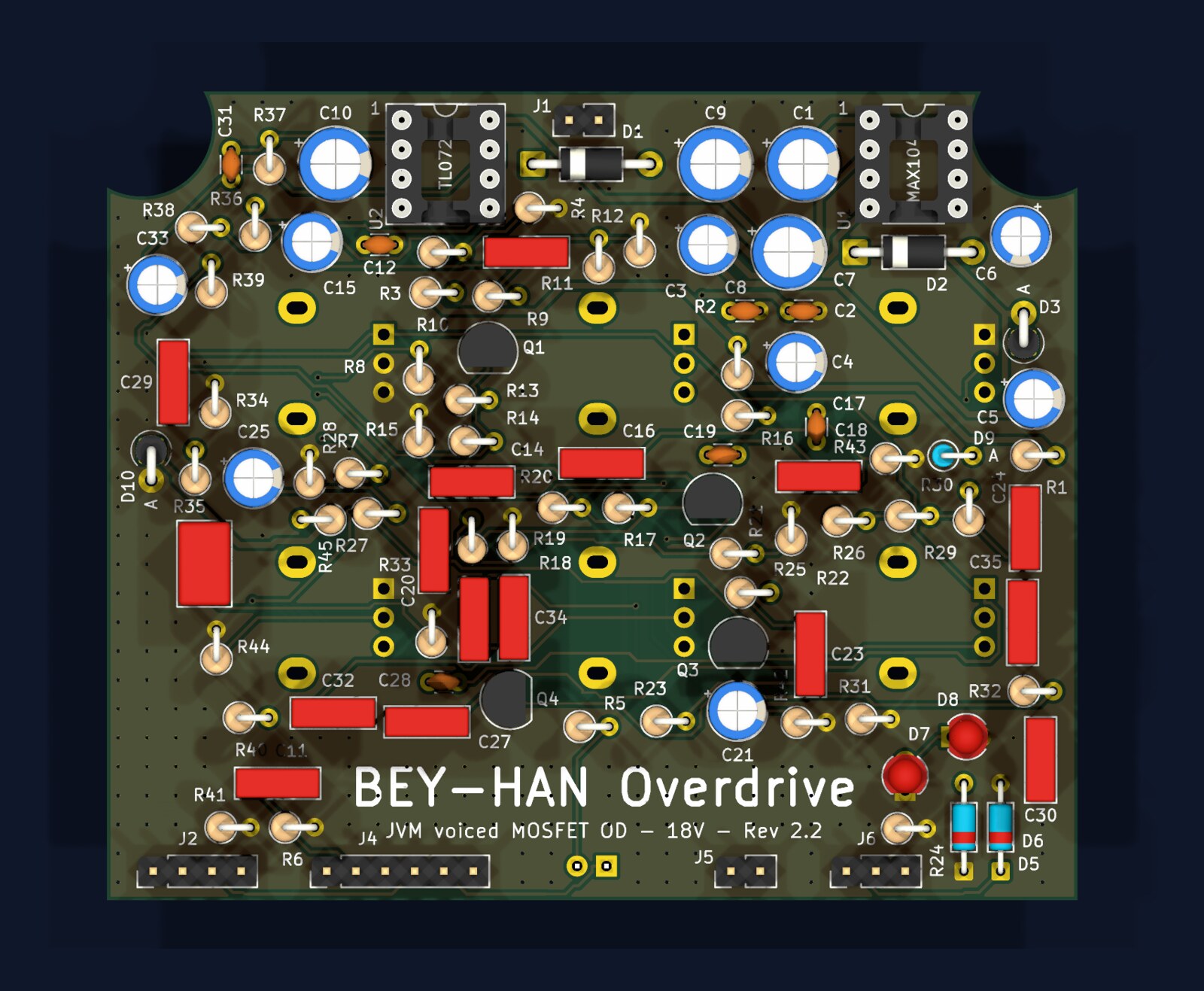
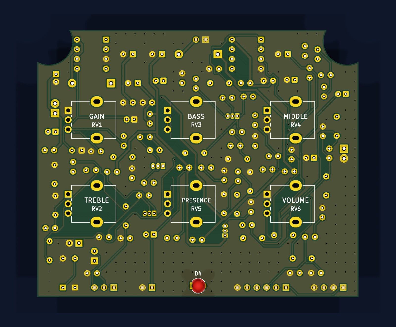
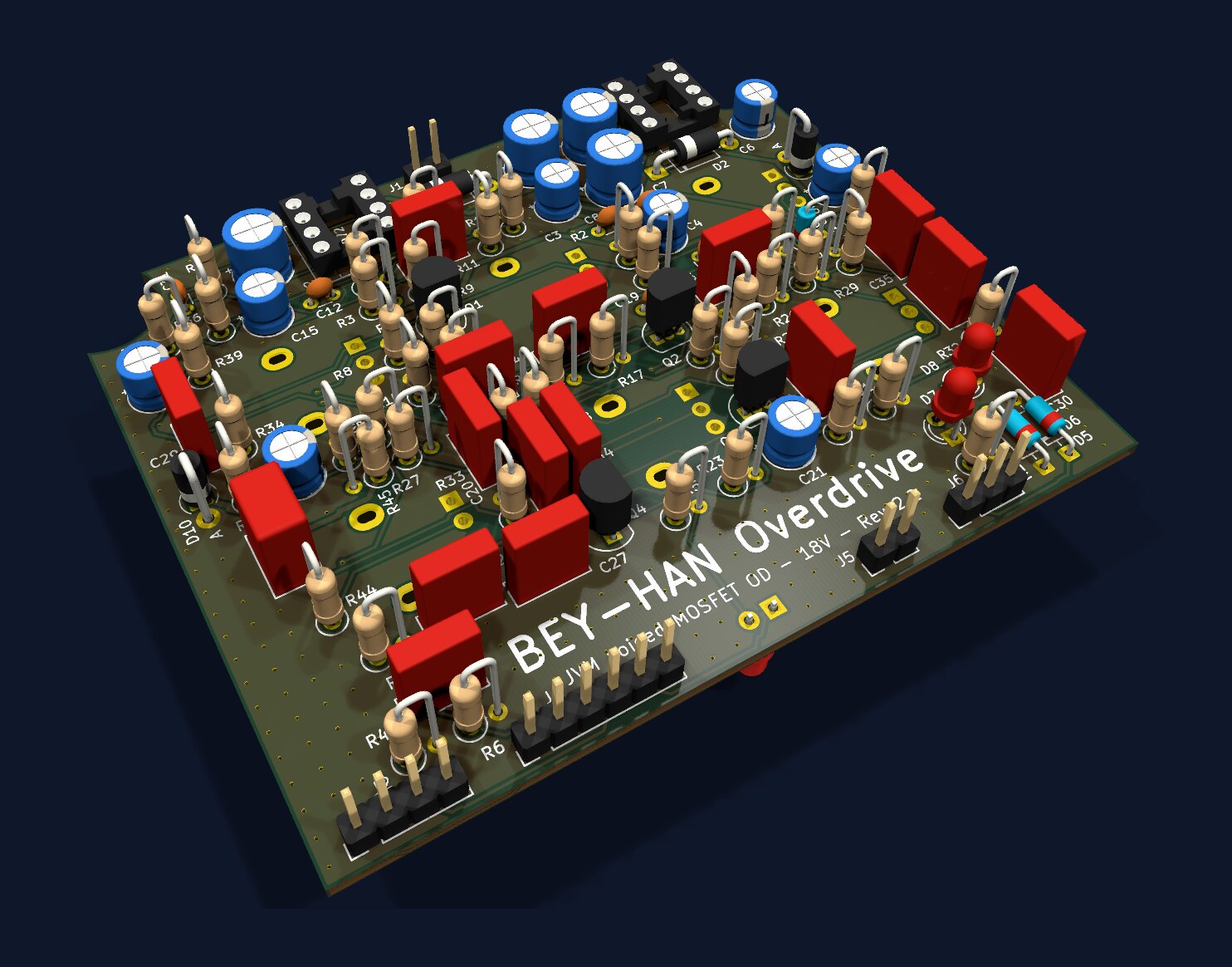
The board is 84 × 70 mm, 1.6 mm FR-4, two layers. All resistors are mounted vertically: it saves space, and it is the only way to fit a 109-part circuit into this size. The ICs sit in DIP-8 sockets rather than being soldered.
The hardest part was mechanical. Inside a 1590BB there is only about a pot body's worth of space, ~7 mm, between the board and the lid. In Rev 1 the pots were on the same side as everything else, and the 11 mm capacitors hit the lid. In Rev 2 I moved the pots and the status LED to the back side: the pot bodies face the lid and every other part faces into the box. Deliberately, no component leads sit under the pots, so the pot bodies sit flat on the board.
Rev 2.2: a reroute
In Rev 2.2 the circuit, parts and values are the same as Rev 2.1; only the copper and the silkscreen changed. I rerouted the board from scratch with fastroute:
- Power traces at least 0.5 mm everywhere. In Rev 2.1, ~29 mm of VCC and ~19 mm of VMOS necked down to 0.15 mm. At a few mA that was no electrical problem, but I widened them for robustness and manufacturing margin.
- An "HV" net class for the 17-18 V nets: V18, PUMP, VCC and VMOS keep at least 0.25 mm from other copper. The one exception is Q4's own legs: with the TO-92's 1.27 mm pitch, drain to gate can only be 0.22 mm, and a custom rule in
beyhan.kicad_druexempts just that. - Notches for the screw bosses: in Rev 2.1 the board's two top corners landed on the box's corner screw bosses. The top corners now have round notches of 6.1 mm radius, sized from Hammond's official drawing plus 0.6 mm for larger bosses on clone boxes and 0.5 mm of position error. To make room, C6 moved to a smaller can, D3 became vertical and C31 went from film to C0G ceramic; the values are unchanged.
- The board sits 1 mm lower in the box: about 1.6 mm of clearance to the top wall and sides. The pot and LED holes moved down 1 mm with it, and the drilling template was regenerated.
- Readable silkscreen: the IC labels moved to the front, and inside the sockets it now says MAX1044 and TL072, with a 1 next to pin 1. Both are DIP-8, and swapping them would put the MAX1044 on 17 V; the silkscreen is there to make that mistake hard.
- Silkscreen lines were thickened to 0.15 mm, JLCPCB's minimum. 161 of the 185 ground stitching vias were kept.
For this post I checked the board again: kicad-cli sch erc reports zero violations, and kicad-cli pcb drc reports zero unconnected pads and a single warning: U1's socket footprint differs from the library copy, because I deliberately removed the socket's outer silkscreen frame, which sat too close to the notch.
Verification
Before ordering boards I tested the circuit in ngspice on a netlist generated from the schematic itself, so the circuit I simulated is exactly the circuit on the board:
| Test | Result |
|---|---|
| DC operating point (BS170 threshold 1.2-3.0 V, OD1 and OD2) | all four stages in saturation |
| Monte Carlo, 40 boards (R ±5%, C ±10%, electrolytics ±20%, each BS170 its own threshold) | no failures, ≥5 V of swing in every stage |
| True bypass | input = output (0.00 dB) |
| Pot direction (clockwise = more) | all six correct |
| Gain range (200 mV input) | OD1: clean up to half the pot, 29% THD near the end; OD2: crunch at 10%, 32% THD |
| Harmonic balance (even / odd) | MOSFET 0.7-1.0, LED 1.0-1.6; Si symmetric (on purpose) |
| Frequency response (tone controls at noon) | slight brightness at 3-6 kHz at low gain, -8 dB at 12 kHz at high gain |
| Current | 5.5 mA on the 17 V rail, ~3 mA on the 9 V rail |
The Monte Carlo run is the real proof of the trimpot-free design: even with each transistor given a random threshold between 1.0 and 3.0 V, the drain voltages stay between 6.6 and 12 V.
Assembly and the enclosure
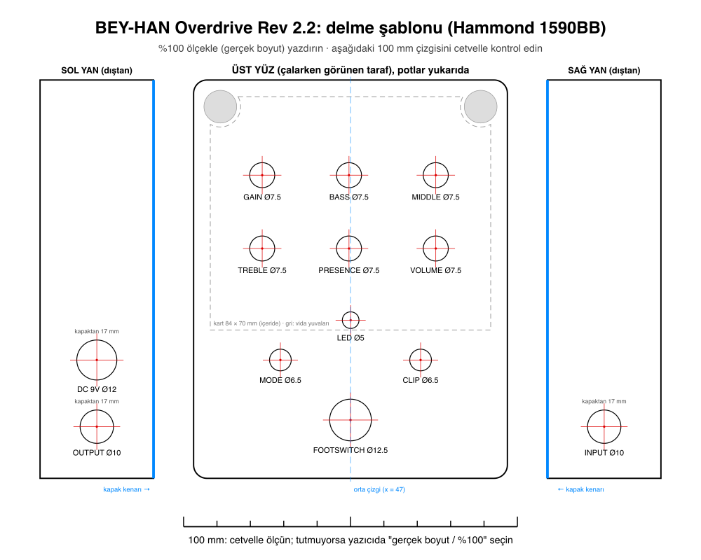
The order package is put together so the pedal can be built from it alone: assembly notes, a parts list (including a spreadsheet for shopping), assembly drawings of both board sides with reference codes and with values, the enclosure drilling template, the footswitch wiring diagram, and the Gerber package to upload to JLCPCB as is. The documents are in Turkish.
First power-up goes step by step: with the ICs out, check that V9 is ~8.4 V; then insert U1 and see VCC rise to 16-17 V; then U2. After that, check the MOSFET drain voltages and that U2's outputs sit around VCC/2. In this order, a mistake gets caught at the first step, before it burns an expensive part.
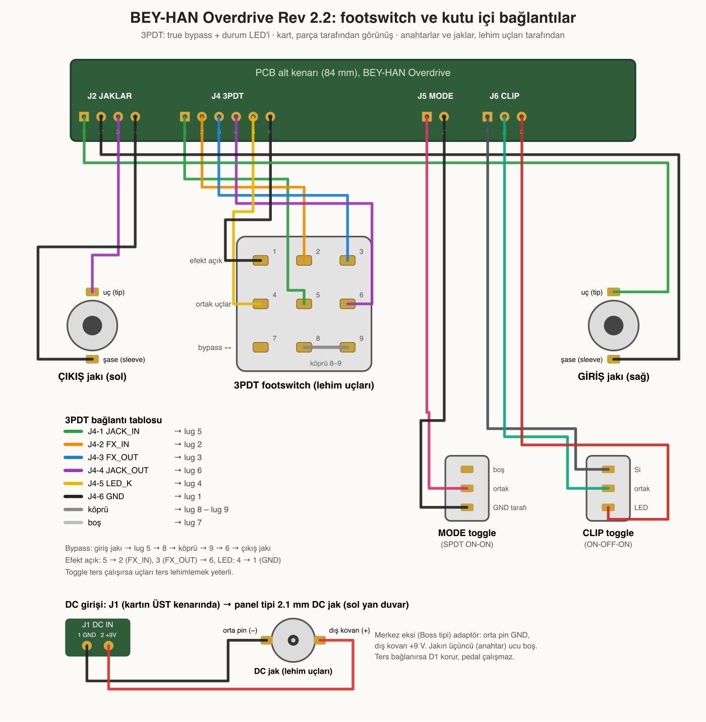
For the enclosure there is a drilling template printed at 100% scale. The 100 mm line on it is checked with a ruler; since clone 1590BB boxes can be 0.5-1 mm larger than Hammond's, the template is aligned to the top edge and centre line of the box.
Choosing parts
- The transistors must be BS170s. The 2N7000 is electrically similar but its pinout is reversed; if used, it has to be rotated 180°.
- The ICL7660S is the safest U1: it tolerates up to 13 V. The MAX1044 works too, but it is marginal when the zener clamp rises to ~10.9 V on a 13 V adapter.
- The electrolytics on the 17 V rail (C6, C7, C9) are 35 V; 25 V parts would have run at 70% of their rating.
- Use a regulated 9 V pedal adapter. The zener protects against short overvoltage, but on a permanent 12 V+ supply it heats up; it is not a permanent fix.
Wrapping up
What pleases me most about BEY-HAN Overdrive is that getting close to a tube sound needed no expensive or exotic parts: four BS170s, the right bias, one resistor change on Q3, and Marshall's tone stack, unchanged for decades. The rest is mechanical patience: moving the pots to the back, notching the corners for the screw bosses, giving the 17 V nets their own clearance rule. The Rev 2.2 order package is ready, with the KiCad 10 source files included.