KAGAN A1: an EL34 tube amp pedal with DSP effects, KiCad files and firmware
A two-stage tube preamp built with MOSFETs, an EL34 power amp and a 4x12 cab sim, followed by eight DSP effects on an STM32G473 and an ES8388. A 6-layer SMD board ready for JLCPCB; the KiCad project, Gerber/BOM/CPL and firmware source are free to download.
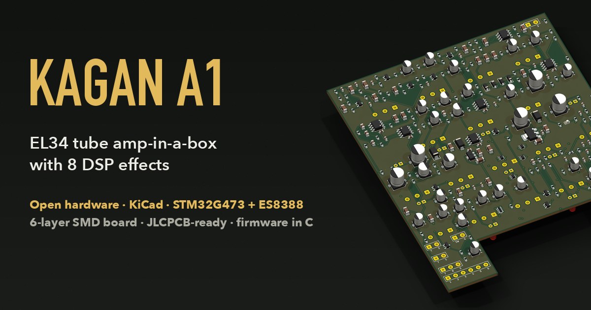
KAGAN A1 is an analog amp-in-a-box that fits a two-stage high-gain tube preamp, an EL34 power amp and a 4×12 cabinet into one pedal enclosure. It needs no computer: it plugs into an audio interface, powered speakers, headphones or the input of a real amp. This post is about the SMD version of the board, which adds a DSP block after the analog amp, built from an STM32G473 and an ES8388 codec: noise gate, phaser, vibe, flanger, chorus, delay, reverb and tremolo.
The KiCad files, Gerber/BOM/CPL and the firmware source can be downloaded at the end of the post.
Signal path
INPUT (1 MΩ) → buffer
 → V1a  2N7002, 680 Ω + 1k‖2.2µ source      [BOOST: +8 dB]
 → GAIN + 100 pF bright
 → V1b  cold clipper (low bias, unbypassed source)
 → V2a  ×5 → V2b source follower
 → passive tone stack: TREBLE / BASS / MIDDLE
 → MASTER
 → EL34 power amp: ×2 (mids) / ×4 (lows, ~100 Hz resonance), PRESENCE,
   symmetric diode clipping (odd harmonics, like push-pull)
 → LEVEL → DSP (gate, phaser, vibe, flanger, chorus, delay, reverb, tremolo)
      ├─ AMP OUT   (no cab sim, into a real amp)
      └─ cab sim: 93 Hz HPF Q1.8 + 5th-order LPF (−19 dB at 6 kHz)
           → LINE OUT, PHONES
The triode stages are built with MOSFETs. Each stage's drain resistor, source resistor and bypass capacitor are chosen to behave like the tube stage it stands for: the 1k‖2.2µ on V1a's source trims the lowest lows, and V1b is a "cold" stage with low bias and no bypass capacitor, the one that gives the amp its characteristic clipping. The tone stack is the classic three-knob passive one (33k, 470p, 22n, 22n; TREBLE and BASS 250k, MIDDLE 25k).
The BOOST footswitch is not in the audio path. It only switches a DC control line, which connects 220 Ω + 22 µF to V1a's source through a MOSFET. A 50 ms RC ramp keeps it from popping.
Simulation
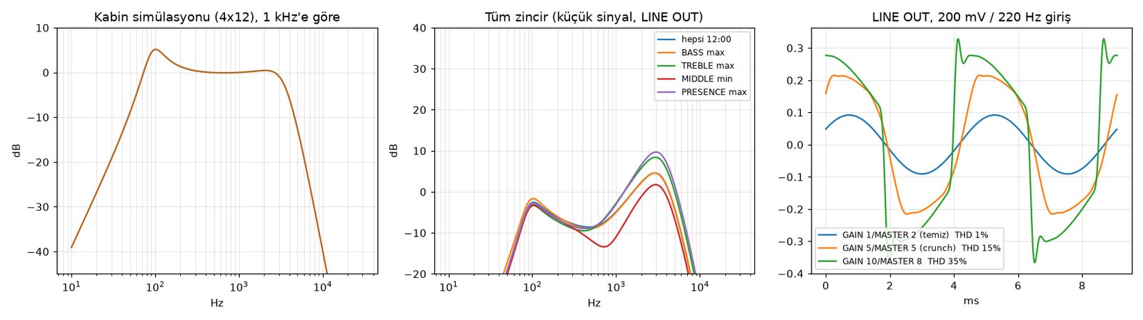
The whole analog circuit is simulated with ngspice (sim/kagan.py). With a 220 Hz, 200 mV input:
| Setting | LINE OUT | THD |
|---|---|---|
| GAIN 1 / MASTER 2 | 65 mVrms | 0.7% (clean) |
| GAIN 5 / MASTER 5 | 166 mVrms | 15% (crunch) |
| GAIN 10 / MASTER 8 | 240 mVrms | 35% |
| GAIN 10 / MASTER 10 / BOOST, 1 V input | 430 mVrms | 39% |
The 2N7002's threshold voltage can be anywhere from 1.0 to 2.5 V. The whole range was simulated and the drain voltages stay in the working region without adjustment. There are no trimmers on the board.
The DSP block
After the LEVEL buffer the signal is halved and goes to the ES8388's left ADC channel. The right channel gets the clean DI signal from the input, and the noise gate decides on that, not on the distorted signal. So the gate looks at how hard the guitar is actually being played, not at the envelope of a clipped, compressed signal.
- MCU: STM32G473CEU6, 150 MHz Cortex-M4F. Most of its 128 KB of RAM goes to the delay line.
- Codec: ES8388, I2S, 24 bit, Fs = 48.828 kHz (12 MHz crystal → PLL → 150 MHz → SAI MCLK 12.5 MHz).
- 32-sample ping-pong buffers over DMA.
- The delay runs at fs/4 and behaves like a BBD: each repeat gets a little darker (2.8 kHz low-pass) and thinner (120 Hz), and saturates softly. Turning D.TIME glides the time over 0.25 s, which gives a tape-like pitch bend.
- The reverb runs at fs/2 and is an 8-line FDN. T60 goes from 1.5 to 3 s with the knob.
- Every effect has one knob and is off with the knob fully left. Over the first 10% of the knob the effect fades in, and phaser, flanger, chorus and vibe are level-compensated: switching them on and off changes the level by no more than ±0.7 dB.
My favourite part is the vibe. In the original Uni-Vibe the four phase-shift stages have different capacitors, and one bulb and its LDRs move them all. The bulb heats up fast and cools down slowly, so the modulation is not a sine but a lopsided throb. The firmware models exactly that:
float drive = 0.5f + 0.5f * sinf(6.2831853f * vb_lfo);
vb_lamp += (drive > vb_lamp ? vb_up : vb_dn) * (drive - vb_lamp);   /* 5 ms heat-up, 25 ms cool-down */
/* LDR: conductance ~ light^0.6, ~2.5 octaves of sweep at full depth */
float m = exp2f(depth * 2.5f * (powf(vb_lamp, 0.6f) - 0.66f));
for (int i = 0; i < 4; i++) {                      /* 90, 240, 1100, 3600 Hz */
    float t = tanf(3.14159265f * VB_F[i] * m / fs_main);
    vb_a[i] = (t - 1.f) / (t + 1.f);
}
Analog bypass
When every effect has been off for 300 ms, the MCU takes the DSP out of the path and the signal goes through the analog route. The same is true at power-up and when the MCU is not programmed: the DSP_EN pin is pulled to ground with 100k. So if the firmware was never flashed, or the codec does not answer, the pedal still works as an analog amp. In simulation both routes have the same gain, and leakage from the inactive route is between −57 and −75 dB.
Knob LEDs
Each DSP knob has a 3 mm LED above it. The level knobs glow with their value (gamma 2.2), the D.TIME LED flashes for 40 ms on every echo, the TREMOLO LED pulses with the tremolo, and the VIBE LED breathes with the virtual bulb. The LEDs are PWM-driven, and the PWM frequency is exactly 2·Fs: 150 MHz / 1536 = 97.66 kHz. If any PWM leaks into the codec through ground, sampling folds it down to DC, so it cannot become an audible tone.
The board
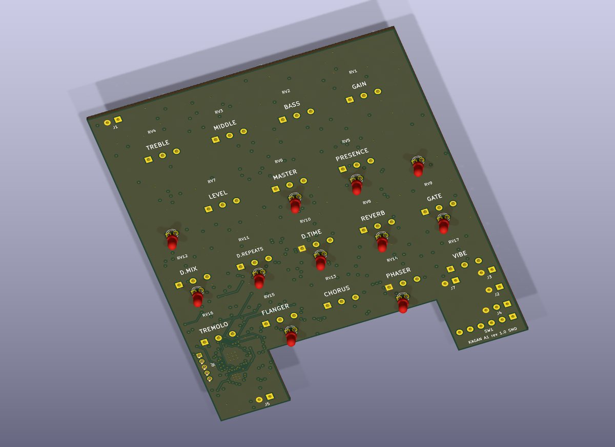
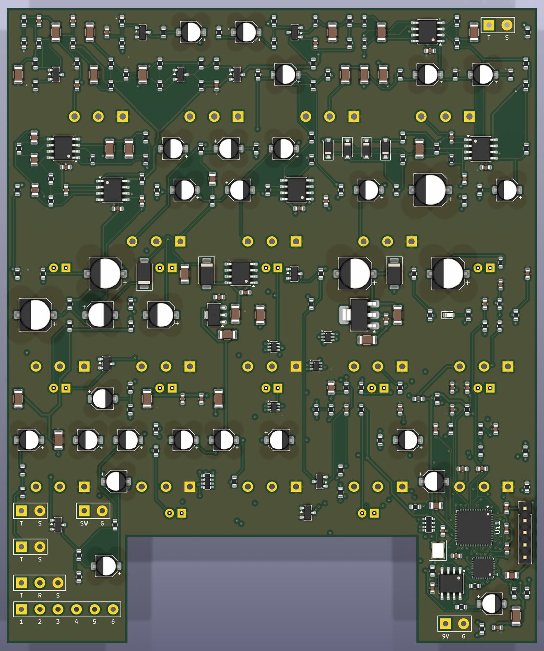
- 110 × 132 mm, 6 layers, Hammond 1590XX enclosure, with a notch at the bottom for two footswitches.
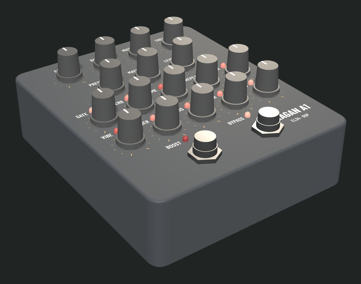
- 17 WH148 pots on the panel side: the top two rows are the analog amp (GAIN, BASS, MIDDLE, TREBLE, PRESENCE, MASTER, LEVEL), the bottom two rows the DSP (GATE, REVERB, D.TIME, D.REPEATS, D.MIX, VIBE, PHASER, CHORUS, FLANGER, TREMOLO).
- Two footswitches: BOOST and a 3PDT true bypass. True bypass covers AMP OUT only. LINE OUT and the headphone output go quiet in bypass, because a raw guitar signal does not sound good in headphones.
- All SMD parts are on the top side, ready for JLCPCB single-sided assembly: 75 distinct parts, 251 placements. 36 parts are soldered by hand (pots, LEDs, wire pads, SWD header).
- Capacitors: C0G in the tone stack, cab sim, presence and resonance paths; X7R/X5R for coupling and decoupling.
The schematic was not drawn by hand. The parts and nets live in a Python file (tools/parts.py), and tools/mksch.py generates the KiCad schematic from it. tools/mkpcb.py places the parts in signal order and then improves the placement with simulated annealing, weighting high-impedance nodes heavily and ground and supply lightly. Routing was done by fastroute, my own autorouter. The result is 0 DRC violations in KiCad, 0 unconnected pads and full schematic parity.
One note: when the board is saved from pcbnew, KiCad resets the project's design rules to its defaults (0.2 mm), and DRC then shows hundreds of violations. The board's rules are 0.15/0.15 mm for the Default class and 0.3 mm for supply nets. Running python3 tools/rules.py before DRC writes them back. The project file in the download already has the right rules.
Firmware
It is written in C without HAL or CubeMX: registers are set directly through the CMSIS headers. The build uses about 19 KB of flash and 103 KB of RAM.
make TOOLCHAIN=/path/arm-gnu-toolchain/bin/   # build/kagan_dsp.bin
make host-test                                # DSP tests on the computer
st-flash write build/kagan_dsp.bin 0x08000000 # with an ST-Link, SWD header J6
make host-test builds the DSP code on the computer and tests it: whether the output is bit-identical to the input with all effects off, the reverb's T60, the delay's timing and repeat ratio, stability at maximum feedback, and level compensation. The tests also write WAV files. The input is not a real guitar recording but a synthetic signal: two notes, heavily clipped, with preamp hiss on top. It is still enough to hear how the effects behave:
- Dry signal
- Full chain: gate + chorus + delay + reverb
- Vibe, Phaser, Flanger, Chorus, Tremolo
- Delay with D.TIME turned while playing, Reverb impulse response
Status
The circuit is simulated, the board is laid out and passes DRC, the firmware builds and the DSP tests pass on the computer. The board has not been built yet. Before ordering:
- Measure the distance from the WH148 shaft centre to the pin row with calipers (the footprint assumes 7.5 mm).
- Check the orientation of every IC, transistor, diode and electrolytic capacitor in the JLCPCB assembly preview.
- At first power-up: the on-board LED should blink at 1 Hz (fast blinking means the codec does not answer on I2C), and with all effects off the DSP route and the analog route should have the same level.
If you build one, I would like to hear how it turns out.
Download
| File | Contents | Size |
|---|---|---|
| kagan-a1-smd-kicad.zip | KiCad 10 project: schematic, PCB, footprints, schematic and assembly PDFs, layer plots, fab files, generator scripts, design notes | 4.2 MB |
| kagan-a1-smd-gerber.zip | Gerber + Excellon only, ready to upload to JLCPCB | 0.9 MB |
| kagan-a1-firmware.zip | Firmware source, Makefile, CMSIS headers, host tests and a prebuilt kagan_dsp.bin | 0.6 MB |
The JLCPCB BOM and CPL files (kagan_smd_bom_jlc.csv, kagan_smd_cpl_jlc.csv) are in the fab/ folder of the KiCad package. The design notes in the package (NOTLAR.md) are in Turkish.